
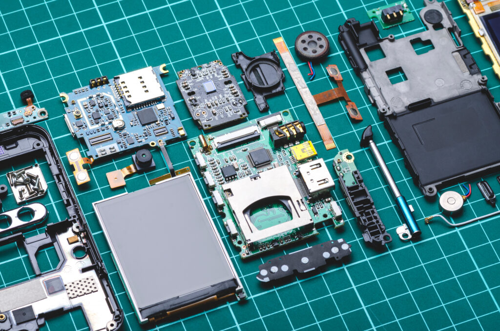
From phones to laptops, home devices to watches, electronic devices – particularly smart devices – have become part of people’s lives, enabling better communication and access to information and making their day-to-day easier.
But the increasing adoption of technology comes at an environmental cost. Electronic devices often have a significant carbon footprint because of the energy-intensive processes needed to produce printed circuit boards (PCBs) and integrated circuits.
Electronics production relies on mining and extracting dozens of different materials, including critical raw materials (economically important materials at high risk of supply shortage, such as lithium or titanium). Extracting these materials has a range of sustainability impacts, including the leakage of toxic chemicals such as cyanide into the environment, high levels of water use, and human rights abuses in the case of ‘conflict minerals’ such as gold and tantalum.
Waste electronic products, or e-waste, is the fastest-growing waste stream in the world, with over 53 million tonnes of e-waste produced in 2019. Most e-waste is disposed of incorrectly, ending up at waste dumps in developing countries. Hazardous chemicals, such as lead or mercury, that may be present in electronic components can leak into the environment, harming local ecosystems and damaging the health of people who live and work in the dumps.
Product sustainability has focused on the circular economy, particularly recycling. But there are fundamental limits to the impact recycling can have on electronics. Only 17% of e-waste is collected for recycling and, even if it’s collected, recovering materials from e-waste is particularly challenging.
Electronics contain trace amounts of rare metals, which are complex and expensive to separate. Only the most abundant materials, such as copper and gold, can be economically retrieved during e-waste recycling, and even if all e-waste was recycled in this way, the material recovered still wouldn’t be enough to meet the growing demands of the industry.
One way to tackle the environmental challenges presented by electronics is to remove the need for them in the first place, for example by detecting a temperature change using a color-changing chemical rather than a sensor. But, in some instances, electronics are necessary, so how can designers reduce the impact of the products they create?
Our sustainability team assessed a range of technologies and design techniques to determine their potential for reducing the environmental impact of electronic products and how difficult they are to implement. This article outlines a few approaches we’ve used in recent projects at CDP.
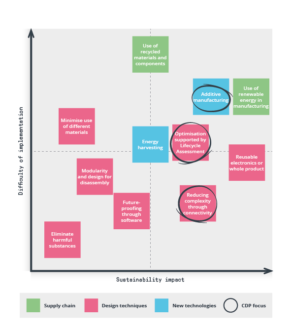
Reducing complexity through connectivity
One of the best ways to reduce an electronic device’s environmental impact is by minimizing the electronics’ complexity, thereby reducing the number of integrated circuits needed as well as the surrounding passive components (resistors, capacitors and so on), connecting tracks, and PCB area.
An easy, effective way to do this is by pairing a product with a user’s existing device to provide the smart capability. Methods range from a simple QR code or NFC chip to a Bluetooth connection for transferring more complex data.
As well as reducing the electronics in the product, this allows for a degree of futureproofing, as software updates can be used to keep the product up to date. This idea isn’t new but is starting to be used more in applications from smart packaging to medical devices.
Important to note: Behind many of these software solutions are large data centers that need powering and should be considered in the product’s environmental impact.
Informed decision-making: Life Cycle Assessment (LCA)
Designers can optimize component choices and circuit designs during detailed design to reduce the overall impact of a product.
We recently used LCA to estimate the additional carbon footprint of adding an electronic module to a medical device. This step allowed our team to identify where to focus on reducing the impact of the design, such as replacing integrated circuits with a solution based on lower-impact passive components and optimizing the layout to minimize the total area of PCB required.
We identified several solutions that together had the potential to reduce the total carbon footprint of the product by up to 25% without compromising functionality. In many cases, this optimization also generates cost savings.
Optimizing electronics through additive manufacturing
Over the past two decades, additive manufacturing (such as 3D printing) has seen a surge in use in mechanical prototyping and manufacture, and its applications in the electronics sector are now starting to grow. In the context of PCBs, additive manufacturing refers to selectively adding conductive material to the areas required, as opposed to a more traditional approach which starts with a layer of copper and selectively etches away the areas where it isn’t needed.
These technologies can improve a product’s carbon footprint through reduced material usage and less energy-intensive manufacturing processes. A report published by the ECOtronics project found, “Changing from subtractive manufacturing (etching) to additive manufacturing (printing) has the potential to reduce environmental impacts by more than 50% across all impact categories.”
One additive manufacturing method is laser direct structuring (LDS), which allows you to construct circuits on the surface of device components. With this approach, you can remove the PCB entirely, dramatically cutting down on the material required.
These technologies present opportunities to fit electronics into new form factors, print onto a wide array of rigid or flexible substrates (the non-conductive part of the circuit board the metal circuit is added to) and increase the customizability of the design, all while reducing the product’s environmental impact.
As we’ve highlighted before, sustainability initiatives should always consider context, which is vital for electronics. In the absence of cost-effective recycling processes, designers must prioritize approaches that reduce the materials and energy required to produce electronics. As electronics continue to play a leading role in our lives, future designs should reduce our reliance on critical raw materials and consider how circular approaches to design can extend product lifetimes and prevent harm to people and the environment.
References
- Conflict minerals used in IT products drive wars and human rights abuses [Internet]. TCO Certified. [cited 19 August 2022]. Available from: https://tcocertified.com/conflict-minerals/
- Global E-waste Monitor 2020 [Internet]. ITU. [cited 19 August 2022]. Available from: https://www.itu.int/en/ITU-D/Environment/Pages/Spotlight/Global-Ewaste-Monitor-2020.aspx
- ECOtronics [Internet]. ECOtronics. [cited 19 August 2022]. Available from: https://www.ecotronics.fi/
Connect with CDP
For more on how to reduce the environmental impact of your electronics through smarter design choices, contact Cambridge Design Partnership.